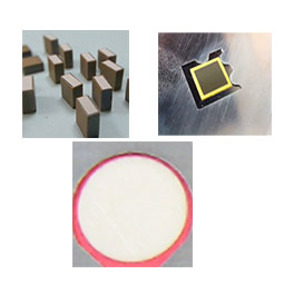
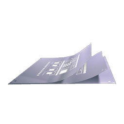
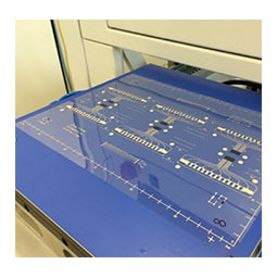
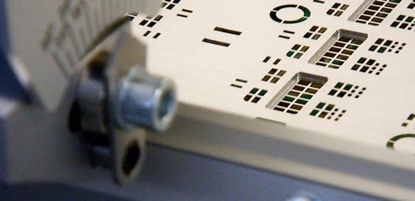
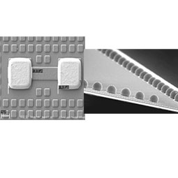
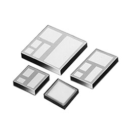
Multilayer Cofired Materials
Using conductive and dielectic layers allows customers to design and product complex circuits with a small footprint. However mostly these materials must also be processed together and therefore need to be able to process under the same conditions most importantly the forming temperatures

MLCI
MLCC
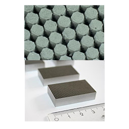
Fuel Cell
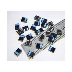
Chip Fuses
Piezo/ PZT
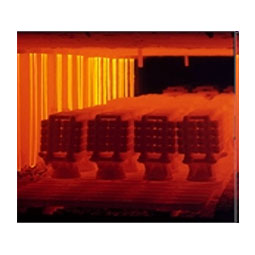
High Temperature Sintering
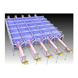
Continuous Oven
LTCC/HTCC
SOFC

Batch Oven
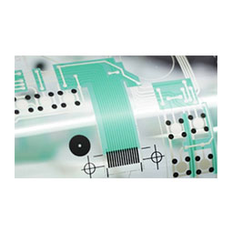
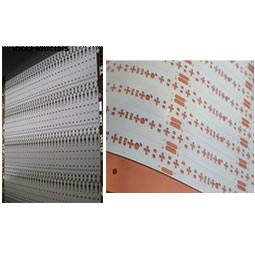
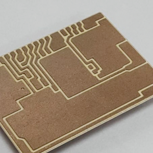
Multi-layer print
Multilayer prints allow the customer to design circuits with crossovers and surface connections with additional building blocks like SMT components to be added to the surface.

Touch Screen

Solar
DBC/ DPC/ TPC
Gas Filters
SOFC
Hybrid circuits
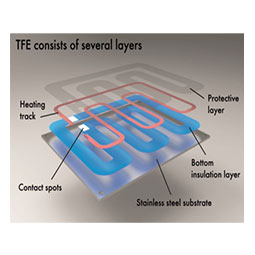
Round Tube Heating/ TFE
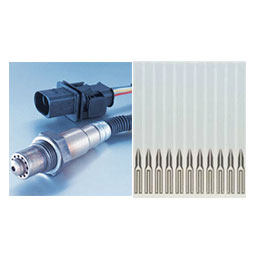
O2/N2 Sensor
Glass
LTCC/HTCC
Chip Fuses
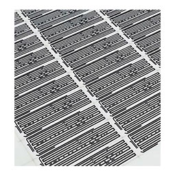
R2R Flexible Electronics
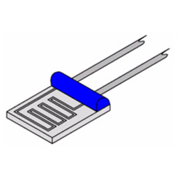
Thick Film Pressure Sensor
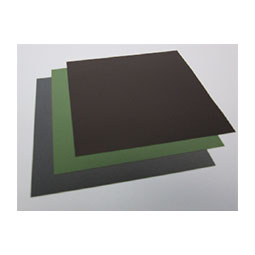
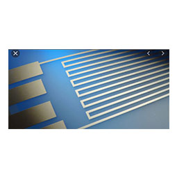
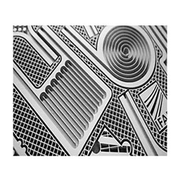
Stencil Print
Stencil print is one of the most economic solutions when producing conductive or dielectric structures. Advantages are in the uniformity of the print and the potential cavities this technology can print in. However other technologies can produce thicker or thinner active and passive layers.
DBC/ DPC/ TPC
Wafer Bumping
LTCC/HTCC
LED Strip Manufacturing
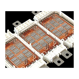
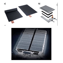
IGBT/ DC-DC/ Power Module

Wafer/ Semiconductor
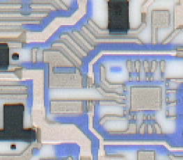
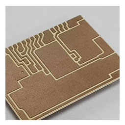
Screen Print
Screen printing is a technology used for creating intricate patterns in a very efficient way. Due to this flexibility and efficiency, the boundries of this technology are constantly being broken down with ever thinner lines and spaces.
Touch Screen
SOFC
Fine Line Metallization
Solar
Piezo/ PZT
Gas Filters
High Temperature Sintering
Micro Tooling
Hybrid circuits
Ceramic wafer High Density Probe Card
MLCC
Glass
LTCC/HTCC

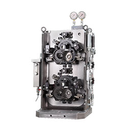
Rotary Screen Printing

Wearable Electronics Manufacturing Equipment
MLCI
Thick Film Pressure Sensor
R2R Flexible Electronics
Chip Fuses
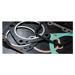
Gasket printing
Round Tube Heating/ TFE
Fluidic Microchannels
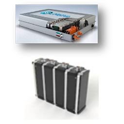
Solid State Battery
Battery
O2/N2 Sensor

Additive / 3D production
Building things from the ground up is in the human nature. However with limited tools we were forced to create some things with destructive methods and create significant waste. Modern design and production tools target to minimize waste and increase efficiency and final products.
High Temperature Sintering
Micro Tooling
Fluidic Microchannels
Solid State Battery
Gas Filters
Piezo/ PZT
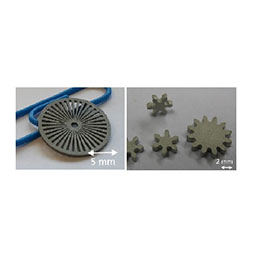
Punching Mechanical Laser
When destructive shaping of products is necessary punching and stampingis often the most precise and economic tool.
In many cases still to today the mechanical punching is the most flexible and fast solution.
SOFC
Hybrid circuits
Piezo/ PZT
Gas Filters
Micro Tooling
Ceramic wafer High Density Probe Card
Glass
LTCC/HTCC
R2R Flexible Electronics
MLCI
Battery
O2/N2 Sensor
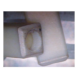
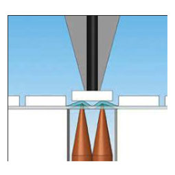
Copper Bonding
Melting two products together can result in the best of two worlds. In the case of copper and ceramic this allows manufacturers to build high power structures which are the basis of our power electronics today.
Hybrid circuits
High Temperature Sintering
DBC/ DPC/ TPC

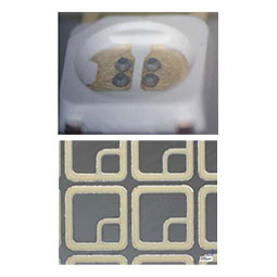
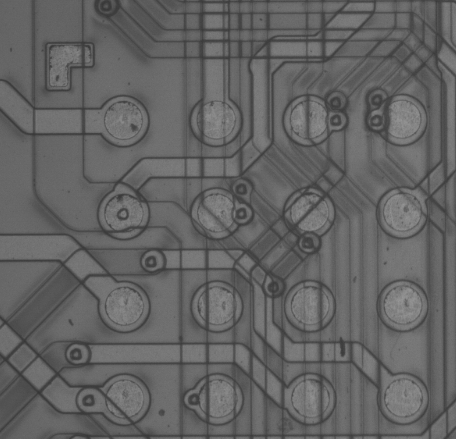
Wafer / Semiconductor
Semiconductors are a core that our electronics are formed around. To shape this core we can use many different tools to design, connect, test and confirm the desired functionality is achieved.
Fine Line Metallization
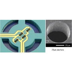
TSV/ Holes/ Vias
Ceramic wafer High Density Probe Card
Surface Rheologie
Dispensing

Reticle
High Temperature Sintering
R2R Flexible Electronics
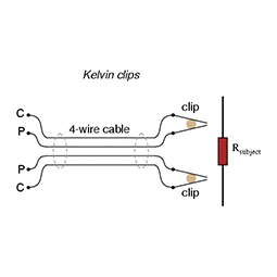
Kelvin Measurement
Rotary Screen Printing
MEMS Micro Mechanical
Glass
Wafer Bumping
Via Filling
Wire Bonding
Die Sorting
LED/ µLED/ Nano LED
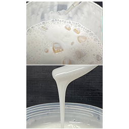
Slurry manufacturing Paste manufacturing
Liquefying materials for the production processes used nearly in every product of our life. Binders and vehicles are mixed with the desired materials and processed to achieve the desired final product shape and parameters such as size, density and thickness.
Fine Line Metallization
SOFC
Hybrid circuits
Micro Tooling
High Temperature Sintering
Slot Die Casting
Piezo/ PZT
Gas Filters
MLCC
Battery
LTCC/HTCC
Doctor Blade Casting
MLCI
Chip Fuses
Ceramic wafer High Density Probe Card
Fluidic Microchannels
Solid State Battery
O2/N2 Sensor
Heat Sensitive Materials Processing
Some materials we like to use in our products are not able to be processed e.g. over 100 C and therefore pose a challenge for processing. UV drying and special inks can still allow customers to implement their designs.
Touch Screen
Fine Line Metallization
R2R Screen Printing
Glass
R2R Flexible Electronics
Rotary Screen Printing
LED Strip Manufacturing
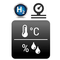
Sensors
Nearly ever product we use today has a sensor to document and react to their environment to create smart devices. Most sensors are exposed to some sort of destructive environment and need to operate in e.g. temperature, acidic, abrasive and harsh environments.
High Temperature Sintering
Hybrid circuits
Piezo/ PZT
Gas Filters
R2R Flexible Electronics
LTCC/HTCC
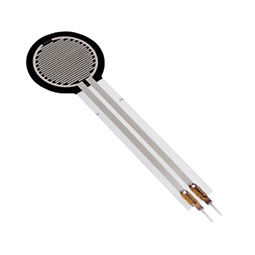
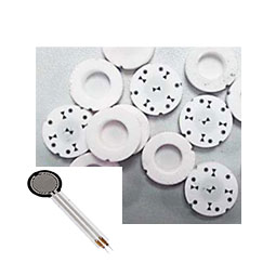
Thinfilm Pressure Sensor
Thick Film Pressure Sensor
Platinum Resistor
Fluidic Microchannels
O2/N2 Sensor

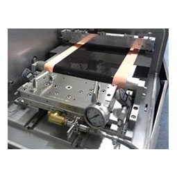
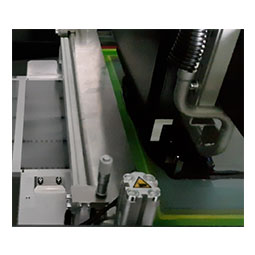
Roll To Roll
One of the biggest challenge of productions is the operator influence. If the processes can be implemented in R2R productions the production efficiency can be increased with less material damages, the throughput can be increased and the overall cost be reduced per circuit.
Fine Line Metallization
SOFC
Solar
MLCC
Thinfilm Pressure Sensor
Glass
LTCC/HTCC
R2R Flexible Electronics
Rotary Screen Printing
Touch Screen
Round Tube Heating/ TFE
Solid State Battery
Battery
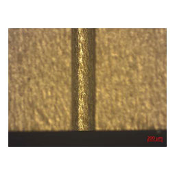
Thin Film
For expensive materials or very specific requirements productions can use thin film processes to create conductive layers. These structures in the meantime also have reached very small sizes but have a lower level of flexibility.
Touch Screen
Fine Line Metallization
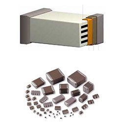
Single layer Capacitors
Thinfilm Pressure Sensor
Platinum Resistor
Glass
R2R Flexible Electronics
Reticle
Wafer/ Semiconductor
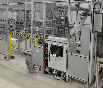
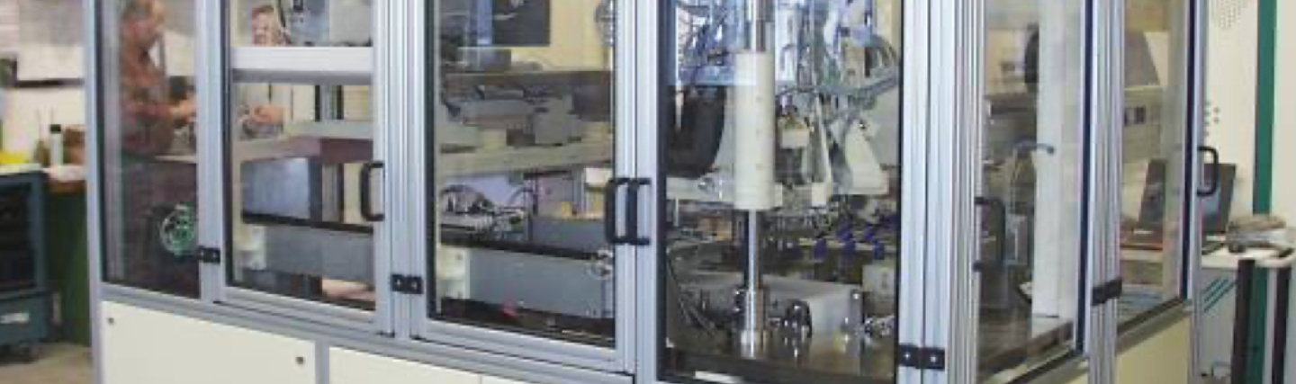
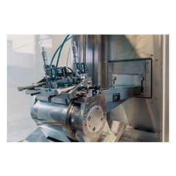
Automation / Assembly
Where economic and necessary processes can be fully automated with present technology. This includes assembly processes, handling, testing and packaging processes.Our partners provide mostly semi-automatic to fully automatic machines even up to smart factories with full live production monitoring.
PEM Cell
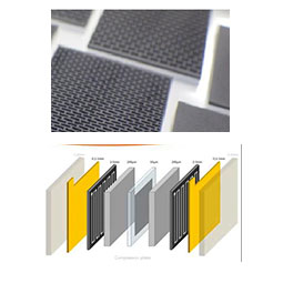
Jigs, Pressure Casting Assembly

Substrates Handling
IGBT/ DC-DC/ Power Module
LED Strip Manufacturing

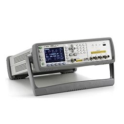
Electrical testing
To confirm functionality electrical measurements are performed on the partial or completed circuits and products. Specialized equipment will allow scrap reduction and product improvements.
Kelvin Measurement
MLCI
MLCC
Single layer Capacitors
Chip Fuses
CAP/ Df measurement
IR measurement
